

_(3).jpg)
Atomic Layer Deposition Market Size
Atomic Layer Deposition Market is anticipated to grow at a CAGR of 12.5% in the forecast period (2024-2034), with the market size valued at USD 2.2 billion in 2023 and projected to reach USD 8.2 billion by 2034.
Product Overview:
Atomic Layer Deposition (ALD) is a method for depositing thin films that enables the precise layering of materials at the atomic level. ALD consists of a series of self-limiting chemical reactions that chronologically deposit thin films onto a substrate layer-by-layer, guaranteeing precision in thickness, uniformity, and material characteristics. This high degree of control and precision makes ALD critical for producing nano-scale components in the semiconductor sector, along with its growing applications in solar energy, medical devices, and battery technology. ALD is especially beneficial for complex, high-aspect-ratio surfaces where alternative deposition techniques are not as efficient. With the ongoing miniaturization of devices across different sectors, ALD technology is experiencing greater adoption for applications that require high precision and dependability.
Market Highlights:
Atomic Layer Deposition Market is expected to exhibit a CAGR of 12.5% during the forecast period, 2024-2034
The Atomic Layer Deposition Market is expected to achieve an overall valuation of USD 8.2 billion, expanding at a CAGR of 12.5% throughout the forecast period due to rising demand for miniaturized electronic components, advancements in semiconductor production, and growing renewable energy applications. With the constant demand for nano-scale precision in gadgets such as smartphones, IoT sensors, and medical implants, ALD's ability to provide uniform, defect-free coatings is essential. Moreover, the global transition to renewable energy has heightened the demand for effective solar cells and battery technologies, in which ALD boosts energy efficiency and longevity. The miniaturization trend in the electronics sector and the increasing investment in nanotechnology are expected to fuel growth in the ALD market, as producers look for precise coating options to match technological progress.
.webp)
Source: Fatpos Global
Atomic Layer Deposition Market Segmentation:
Thermal ALD leads the market due to its effectiveness in producing high-quality, uniform films
The Atomic Layer Deposition Market is bifurcated based on the Product into Thermal ALD, Metal ALD, Plasma-enhanced ALD, and Others. Thermal ALD is the leading category in the ALD market. It is commonly used due to its efficiency in creating high-quality, uniform, and conformal thin films on an atomic scale. This technique depends on successive chemical reactions that take place at moderate temperatures, rendering it appropriate for a wide variety of substrates and materials, such as semiconductors and solar cells. Thermal ALD is favored in semiconductor fabrication, as accurate and uniform layer deposition is essential for developing complex structures at the nanoscale. Its proven reliability and adaptability have set it as the benchmark in ALD, especially for applications that demand layer consistency, like transistors and capacitors in microelectronics.
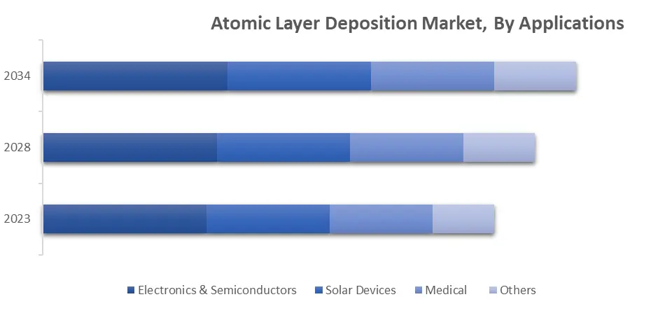
Electronics & Semiconductors lead the market due to advancements in semiconductor miniaturization and complexity
The Atomic Layer Deposition Market is divided based on Applications in Electronics & Semiconductors, Solar Devices, Medical, and Others. The electronics and semiconductor segment tends to hold the leading market position owing to the constant technological developments in the miniaturization and complexity of semiconductor devices. ALD plays a vital role in creating ultra-thin and accurate layers, which are essential for advancing next-gen semiconductors, such as 3D NAND, DRAM, and FinFET technologies. The accuracy and consistency provided by ALD make it essential in this particular segment, as it guarantees superior performance traits for transistors, capacitors, and other vital parts. As the demand grows for compact, powerful devices such as smartphones and wearables, ALD's importance in semiconductor manufacturing is swiftly increasing, enabling the creation of energy-efficient and higher-density components.
Market Dynamics:
Growth Drivers
Rising Investment in Nanotechnology to Propel Market Growth
The ALD market is propelled by the rapid developments in nanotechnology, which plays a vital role in sectors such as automotive, aerospace, and defense. With these sectors progressively depending on tiny devices and nanostructured materials, the precision of ALD's layer-by-layer deposition becomes essential. ALD facilitates the creation of coatings with uniform atomic thickness, vital for uses such as fuel cells, sensors, and electronic parts. The distinctive ability of ALD to produce high-quality films on complex shapes fuels its demand as these sectors aim for compact yet highly effective components. The growing range of nanotechnology research and applications is expected to boost ALD utilization as sectors strive to advance material science and reduce device size.
Demand for Advanced Semiconductor Technologies to Fuel Market Expansion
As the demand for powerful, efficient, and compact electronic devices grows, there is a considerable requirement for precise manufacturing methods such as ALD. This technique offers unparalleled control at the atomic level, crucial for creating advanced semiconductor parts at nanoscale sizes. With the advancement of semiconductor technologies toward smaller nodes, ALD’s ability to produce ultra-thin, conformal films free of defects is essential for the manufacturing of transistors, capacitors, and memory chips. With the rise of 5G, IoT, and AI technologies in various industries, the need for ALD in semiconductor production is projected to keep increasing, bolstered by funding in advanced electronics.
Restraints
Technical Complexity and Process Limitations May Hinder Market Growth
While ALD provides precise control, it also creates difficulties regarding process complexity and restrictions in deposition rates. The stepwise, self-limiting characteristics of ALD reactions result in extended deposition times, which may impede its effectiveness for high-throughput production requirements, particularly in sectors where swift manufacturing is essential. Moreover, the elevated temperatures typically needed for thermal ALD may restrict its use to specific substrates. These technical constraints limit the variety of materials that can be effectively utilized with ALD, affecting its scalability and raising expenses for industries that demand both speed and accuracy in production. Overcoming these technical challenges will be essential for enhancing ALD’s involvement in wider manufacturing uses.
Recent Developments
- Lam Research Corporation has focused on expanding its ALD product lineup to support emerging semiconductor applications, focusing on smaller node processes. The company has entered into recent partnerships with leading semiconductor manufacturers to drive innovation in advanced ALD applications.
- ASM International has released a new thermal ALD system aimed at next-generation semiconductors, designed to improve throughput and reduce material waste. The company has entered into a joint venture with a leading research institute to explore ALD applications in nanotechnology.
- Applied Materials introduced a high-speed ALD tool for semiconductor manufacturing, focusing on enhancing scalability for 5nm and below processes. The company has strengthened its presence in Asia-Pacific through a partnership with regional chipmakers to advance ALD for 3D NAND and DRAM technologies.
- Picosun Group launched a specialized ALD solution for medical devices, enhancing coating precision for biocompatible implants. The company has also recently collaborated with a solar energy firm to develop ALD coatings aimed at improving photovoltaic efficiency.
Atomic Layer Deposition Market: Key Players:
- Lam Research Corporation
- Forge Nano
- ASM International
- Applied Materials, Inc.
- Picosun Group
- Tokyo Electron Limited
- Kurt J. Lesker Company
- Veeco Instruments Inc.
- Beneq Oy
- Encapsulix
- Oxford Instruments
- Sentech Instruments GmbH
- Aixtron SE
- Hitachi High-Tech Corporation
- Other Prominent Players (Company Overview, Business Strategy, Key Product Offerings, Financial Performance, Key Performance Indicators, Risk Analysis, Recent Development, Regional Presence, SWOT Analysis)
Regional Analysis
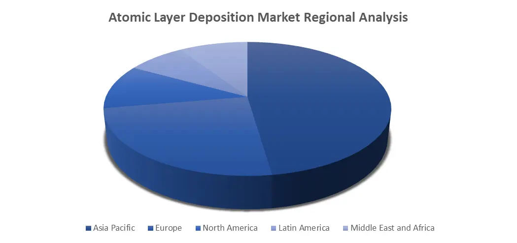
The Atomic Layer Deposition Market is segmented based on regional analysis into five major regions: North America, Latin America, Europe, Asia Pacific, and the Middle East and Africa. The Asia Pacific region tends to dominate the market, propelled by the significant number of investments made in semiconductor production and electronics. Larger economies such as China, South Korea, and Japan host some of the largest semiconductor producers globally, with many being the early implementers of cutting-edge ALD technology. The increasing output of consumer electronics and electric vehicles in China and India additionally drives the demand for ALD in areas such as battery and solar cell manufacturing. The strong industrial foundation of the Asia-Pacific region, along with governmental support for technology and renewable energy, bolsters its leading position in the ALD market.
North America and Europe hold a substantial share of markets, particularly in semiconductor research and development as well as renewable energy. North America, especially the U.S., hosts leading ALD equipment producers, whereas Europe’s strong focus on sustainable technologies fosters ALD expansion in the solar and battery industries. Despite being emerging regions, Latin America, the Middle East, and Africa currently have minor roles owing to inadequate infrastructure and reduced investment in nanotechnology and advanced manufacturing.
Source: Fatpos Global
Impact of Covid-19 on Atomic Layer Deposition Market
The COVID-19 pandemic has had a diverse impact on the ALD market, as global supply chains experienced delays and reductions in production output due to lockdowns and restrictions. The production and installation of ALD equipment were affected, leading to delays in numerous semiconductor and electronics projects. Nevertheless, as industries adjusted to new standards, the demand for electronics, healthcare equipment, and renewable energy surged, particularly due to the heightened dependence on digital gadgets and telecommunications systems. The pandemic has highlighted the requirement for robust supply chains and accelerated investments in localized semiconductor manufacturing, which will positively impact the ALD market in the long run. The sector's rebound has been strong, featuring ongoing advancements in ALD uses throughout various industries.
Atomic Layer Deposition Market is further segmented by region into:
- North America Market Size, Share, Trends, Opportunities, Y-o-Y Growth, CAGR – United States and Canada
- Latin America Market Size, Share, Trends, Opportunities, Y-o-Y Growth, CAGR – Mexico, Argentina, Brazil, and Rest of Latin America
- Europe Market Size, Share, Trends, Opportunities, Y-o-Y Growth, CAGR – United Kingdom, France, Germany, Italy, Spain, Belgium, Hungary, Luxembourg, Netherlands, Poland, NORDIC, Russia, Turkey, and Rest of Europe
- Asia Pacific Market Size, Share, Trends, Opportunities, Y-o-Y Growth, CAGR – India, China, South Korea, Japan, Malaysia, Indonesia, New Zealand, Australia, and Rest of APAC
- Middle East and Africa Market Size, Share, Trends, Opportunities, Y-o-Y Growth, CAGR – North Africa, Israel, GCC, South Africa, and Rest of MENA
Atomic Layer Deposition Market Scope and Segments:
|
ATTRIBUTE |
DETAILS |
|
Study Period |
2018-2034 |
|
Base Year |
2023 |
|
Forecast Period |
2024-2034 |
|
Historical Period |
2019-2022 |
|
Growth Rate |
CAGR of 12.5% from 2024-2034 |
|
Unit |
Value (USD Billion) |
|
Segmentation |
Main Segments List |
|
By Product |
|
|
By Application |
|
|
By Region |
|
Frequently Asked Questions (FAQ):
Atomic Layer Deposition Market size was valued at USD 2.2 billion in 2023 and is projected to reach the value of USD 8.2 billion in 2034, exhibiting a CAGR of 12.5% during the forecast period.
The Atomic Layer Deposition (ALD) Market involves a thin film deposition technique that enables precise control over film thickness and composition, crucial for semiconductor, solar, and medical device manufacturing. ALD enhances performance, efficiency, and reliability in various applications, driving demand in industries requiring nanoscale material deposition.
The Thermal ALD segment and Electronics & Semiconductor ssegment accounted for the largest Atomic Layer Deposition Market share.
Key players in the Atomic Layer Deposition Market include Lam Research Corporation, Forge Nano, ASM International, Applied Materials, Inc., Picosun Group, Tokyo Electron Limited, Kurt J. Lesker Company, Veeco Instruments Inc., Beneq Oy, Encapsulix, Oxford Instruments, Sentech Instruments GmbH, Aixtron SE, Hitachi High-Tech Corporation and Other Prominent Players.
Increasing demand for miniaturization of semiconductor devices, rising adoption in renewable energy and medical devices, and advancements in ALD technology are driving the Atomic Layer Deposition Market.
 Select License Type
